Perovskites for solar energy conversion
Hybrid trihalide perovskites (e.g. methylammonium lead halides CH3NH3PbX3, where X = I or Br) (Structural figure below) have been demonstrated to be a potentially disruptive technology for third generation photovoltaics. Impressive lab-scale advancements in increasing the power conversion efficiency (PCE) – from approximately 4% to over 25% – have been achieved through optimization of the active layer fabrication and engineering of interfaces within photovoltaic devices [1]. However, the large-scale utilization of this class of materials and private-sector investments are still hampered by critical limitations: i) the inherent instability in air and hysteretic behavior of devices, and ii) the inhomogeneity of the perovskite thin films (both in terms of continuity and of structural and electrical properties at the nanoscale). Addressing current limitations of this material has the potential to meet society’s great need for lowering our carbon-footprint and expanding the installation of efficient and affordable renewable energy technologies.
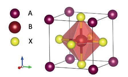
Fig. 1. A schematic of a perovskite crystal structure. Perovskite compounds typically have a chemical formula ABX3, where ‘A’ is a monovalent organic or inorganic cation, ‘B’ represents Pb or Sn cations and X is a halide anion (I, Br, or Cl).
While there has been promising progress over the past few years, challenges specifically in understanding and controlling the presence of heterogeneities in thin films of novel materials must be overcome. Although solution-based synthesis routes offer process simplicity, scalability, and low temperature processing, limited control over how atoms and molecules in solution assemble into macroscopic functional thin films can negatively affect optoelectronic performance. In particular, solution-processed thin films are typically polycrystalline, and therefore, consist of electronic and crystallographic defects. Our research aims at developing fundamental understanding and control of how reactants assemble into products and how this transformation influences the functional properties and stability across the thin film.
Chemical solution synthesis is chosen to fabricate thin films due to its highly flexible character including the relative process simplicity, low-cost deposition equipment, and the compatibility with large area high throughput processing. The precursor solution preparation involves chemical precursor selection and choice of a solvent or solvent system. Chemical additives may be added to the precursor solution to facilitate or reduce chemical reactivity. Depending on the reagent and solvent choice as well as solution reaction conditions homogeneous molecular level mixing of reagents can be achieved.
Heterogeneities appear in various materials on different length scales (atomic level to hundreds of micron) almost irrespective of deposition technique. These heterogeneities occur because of challenges in fully controlling solution synthesis and are commonly a detriment to electronic properties. For example, some heterogeneities may serve as traps for charge carriers or degradation sites [2]. However, in some systems such as halide perovskites, heterogeneities can be beneficial, serving for example to improve solar conversion efficiency [3]. Thus, our goal centers around the understanding and controlling the effects of heterogeneity on functional properties on different length scales rather than achieving homogeneous films. Examples of heterogeneities on different length scales are shown in Fig. 2.
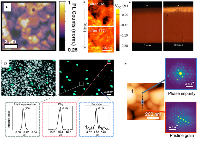
Fig. 2. Exemplary overview of heterogeneities in halide perovskites revealed by different probes and spanning atomic to um-scale length scales. a) Photoluminescence image overlaid with a scanning electron microscope image; b) Map of absolute open-circuit-voltage under 1-sun; c) Optical images of halide perovskite material across a lateral device (channel width 75 mm) showing the material changes close to the anode side; d) Photoemission microscope image and correlated nano-X-ray diffraction measurements; e) atomic force microscopy image overlaid with photoemission microscope image [6].
The model system to develop the full methodology on are halide perovskites because they are currently the most promising photovoltaic (PV) material on the market [1] as well as emerging in photoelectrochemical devices [4]. Moreover, there is promise that halide perovskites can further reduce the cost of photovoltaics by combining perovskites with well-established Silicon cells by adding only little to the overall cost. This class of materials is mostly processed with solution synthesis resulting in high quality materials although spatial compositional and structural heterogeneities were reported [2], [5]. Despite the high performance of halide perovskites, the evolution and in particular control of heterogeneities related to characteristically large defect densities affecting the optoelectronic performance is not well understood [2], [3]. Furthermore, local nanophase impurities were recently linked with stability losses, which is the major hurdle before commercialization of the halide perovskite technology can happen. We hypothesize that microscopic heterogeneities significantly affect material stability, thereby effectively altering the electronic behaviors of photodoping/tunneling and trapping.
Overcoming the challenge of contacting non-uniform films, terahertz time-domain spectroscopy (THz-TDS) is a very powerful probe of conductivity and transport properties in non-contact mode. In addition, it also avoids making a device to characterize film properties that might be obscured by imperfect contact formation. Terahertz spectroscopy can sense the frequency-dependent conductivity over a broad range of frequencies, which permits the matching of data using microscopic models and extracting critical parameters such as carrier density, mobility, diffusion length, scattering times, and effective mass of carriers.
To address how the heterogeneous structure of perovskites affects the optoelectronic function, we will combine measurements from terahertz and optical spectroscopy with photoconductive scanning probe microscopy to permit spatial mapping of conductivity and other properties within the resolution of the probe wavelength. The visualization of maps with terahertz frequencies will be correlated with maps of photoluminescence, transmission, and transient absorption in the visible and near-infrared regimes. Such mapping correlations will help provide a more complete picture by combining perspectives on how connects heterogeneity at different length scales in perovskite structures connect in perovskite structures to conductivity properties and will also serve as valuable insights for initiating and validating the structure-property predictions from theory. In our studies, we hope to understand the role of grain boundaries, defects, and strain on optoelectronic properties. The laboratory at CSUEB is well-equipped for a variety of measurements of thin-film materials, including terahertz time-domain spectroscopy, and in the optical regime both time-resolved photoluminescence and transient absorption experiments.
[1] “Best Research-Cell Efficiency Chart | Photovoltaic Research | NREL.” https://www.nrel.gov/pv/cell-efficiency.html (accessed Aug. 21, 2022).
[2] S. Macpherson et al., “Local nanoscale phase impurities are degradation sites in halide perovskites,” Nature 2022 607:7918, vol. 607, no. 7918, pp. 294–300, May 2022, doi: 10.1038/s41586-022-04872-1.
[3] E. M. Tennyson, T. A. S. Doherty, and S. D. Stranks, “Heterogeneity at multiple length scales in halide perovskite semiconductors,” Nature Reviews Materials 2019 4:9, vol. 4, no. 9, pp. 573–587, Jul. 2019, doi: 10.1038/s41578-019-0125-0.
[4] V. Andrei, B. Reuillard, and E. Reisner, “Bias-free solar syngas production by integrating a molecular cobalt catalyst with perovskite–BiVO4 tandems,” Nature Materials 2019 19:2, vol. 19, no. 2, pp. 189–194, Oct. 2019, doi: 10.1038/s41563-019-0501-6.
[5] K. Frohna et al., “Nanoscale chemical heterogeneity dominates the optoelectronic response of alloyed perovskite solar cells,” Nature Nanotechnology 2021 17:2, vol. 17, no. 2, pp. 190–196, Nov. 2021, doi: 10.1038/s41565-021-01019-7.
[6] S. D. Stranks, “Multimodal microscopy characterization of halide perovskite semiconductors: Revealing a new world (dis)order,” Matter, vol. 4, no. 12, pp. 3852–3866, Dec. 2021, doi: 10.1016/J.MATT.2021.10.025.
